
This is a copy of the recreation that used to be hosted at http://projectspeccy.com/projects/ with permission from Steve SmithA while ago, I remembered what fun I had on the Sinclair Spectrum, an AT&Y SPEC-MATE and Microdrives, hacking games for infinite lives and such. Sadly, try as I might, I can’t find a SPEC-MATE for sale anywhere. This led me onto the Multiface. A device produced by a company called Romantic Robot. With one attached, the user is able to freeze a program, save it to a variety of formats (Tape, Microdrive, Disk etc.) and add ‘pokes’ (change RAM values) for said infinite lives.
I first tried to re-create a simpler interface, the Spanish Phoenix III. My prototype appears to work with the Phoenix ROM but can’t page out at the moment. It also seems to work with the SPEC-MATE ROM but with the same issue. Research on that one continues.
In the meantime, I sought to investigate how these interfaces work and see if I could re-create one from the hardware itself. I chose to work on the Multiface 128 since it is compatible with the 48K/128K and +2 models of Spectrum, and I am in contact with someone re-creating the Multiface 3, which is compatible with the +2A/B and +3 models. Between us, all the models are covered!
I have been made aware that there are several issues with the Multiface 128 design I have chosen to copy. However, I copied it verbatim for an authentic re-creation.
The first step was to photograph the board in detail to use as a reference for re-building later and for chip placements etc. I will post the images I captured along with the design files below.
Following this, I stripped my Multiface down to bare board. I acheived this using a de-solder gun, a most useful piece of equipment. I tried very carefully to de-solder all the chips without damage. Sadly, the 74LS27 was very stubborn and got a bit mangled! On the positive side, the PCB wasn’t damaged at all during the process which means I should be able to re-build the interface at a later date.
I placed all the chips on an non-conductive sponge in a box, along with the rest of the components. The only part I didn’t remove was the edge connector and passthrough board. This would have been a difficult job to do without causing unnecessary damage.
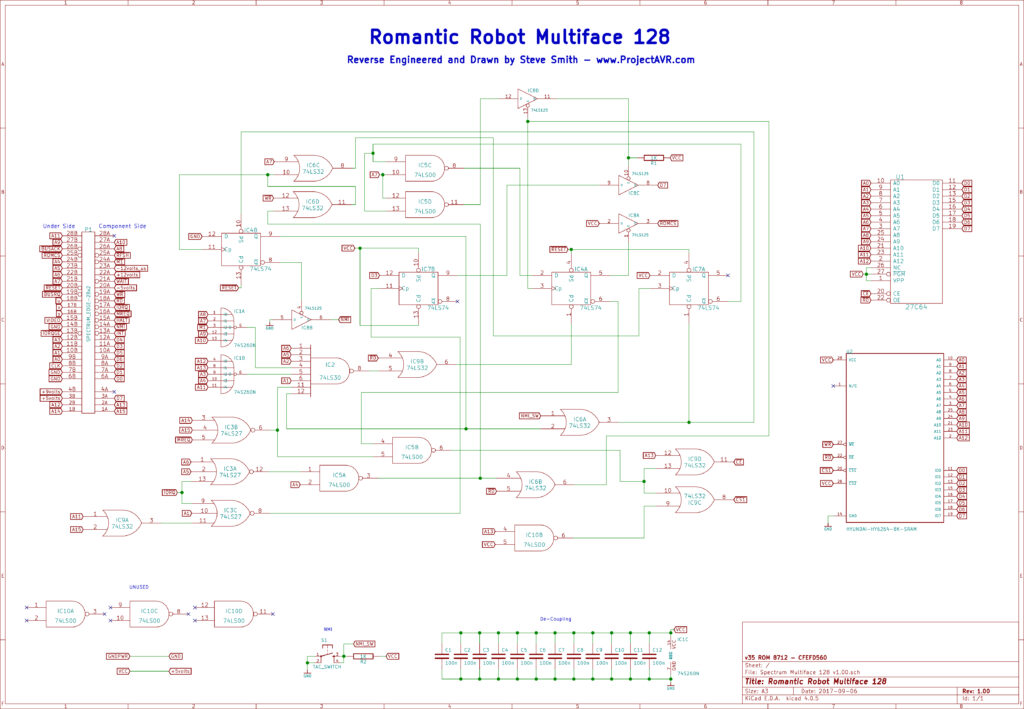
I then proceeded to lay out a set of components in the EDA Program KiCad. A free Schematic capture and PCB Layout program. I recently converted from EagleCAD, and I have grown used to the different methodologies without too much difficulty. Once I had laid out a full set of components, some of which I had to draw from scratch, I added the connections for the edge connector. I prefer to use net labels to indicate connections rather than the more conventional bus lines. I find it makes for a cleaner diagram.
When I had completed the edge connector, I traced each connection along it. I started with the upper connections since they were easier to access. I followed the tracks with a pointing device, in this case a pencil! Where I was unsure a connection got to a particular destination due to interconnecting vias, I would double check with a multimeter set on it’s lowest resistance range. Most modern meters have a continuity/diode check that can be used for this purpose. My aged Fluke 73 has to make do with resistance ranges.
This process was quit painstaking but essential to get correct. Lots of the connections go to more than one chip’s pin so checking multiple times is essential. When I had gone through all the edge connector connections, I continued by tracing every chip pin one by one. The board isn’t marked so I added my own component designations to one of the images I had captured and copied those in KiCad.
Each chip pin was traced and gradually, I assembled the circuit diagram, line by line. Again, checking, double-checking, and even triple-checking were necessary to avoid mistakes. After all the chips were done, I added the two resistors, NMI button and the protection diode on the edge connector. This diode is omitted on the prototype since I didn’t intend to put a passthrough on it, but it can easily be added. Finally, after a good few man-hours, the job was done.
Time to design a PCB. I intended to get the prototype PCBs fabricated by EasyEDA due to the fairly fast turnaround and good price point for prototype boards. The final boards I will have made by Hackvana since they are of very high quality. To hit EasyEDAs Prototype price point, the PCBs needed to be within 100mm x 100mm in size. The original Multiface board is 114mm x 70mm, so I shuffled it around slightly. Later on I will expand the board out to fit the original case.
The PCB was quite challenging to lay out. It required mutiple vias and some creative routing. I hand routed all of the connections one by one. This is my favorite part of any design though.
Having routed the board, I did a DRC check to make sure the connections were all complient with the design rules I had set up. All was fine. I then plotted Gerbers and drill files which would be submitted to the fabricator. Rather than trust these files are OK, it’s good practice to check them externally to KiCad. I use Gerblook at the moment but I have noticed a message on the site to say it has been bought. Hopefully the service will remain free of charge.
Having checked the board looked correct on Gerblook, I uploaded the ZIP of Gerber files and drill file to EasyEDA and ordered the prototype boards. Time passes….
…And the boards arrive. they took around 2 weeks from the time I ordered them. Not bad for a budget service.
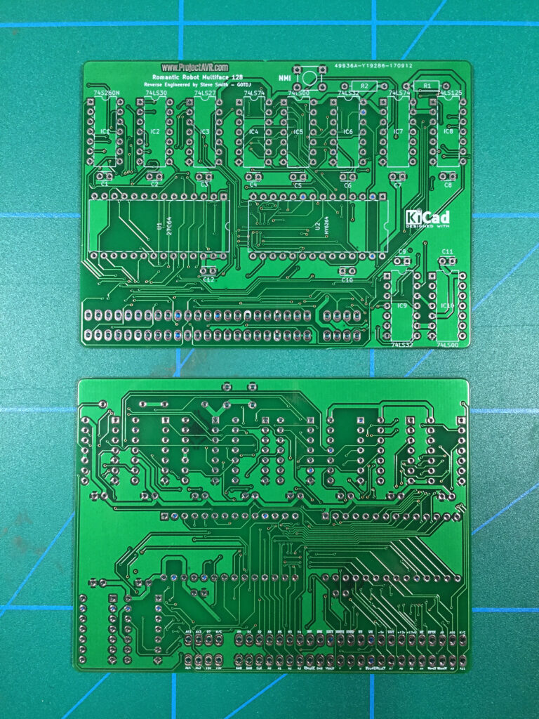
A quick visual check found the boards in good order. I assembled all the components, including a few from the original device since I had none of those particular ones in stock. I soldered the de-coupling capacitors first since they are the lowest profile. I followed these with the resistors and NMI button, then all of the chip sockets.
The above image is the completed interface mounted on the rear of a 48K Spectrum Plus. You will note that the edge connector faces the Spectrum and the chips are on the reverse of the board. This is in keeping with the original design. It also means that the board has extra room behind between it and the Spectrum. You will also notice that the ROM chip U1 has no Erase window. This is because I had no 27C64 EPROMs in stock. This is an OTP chip (One Time Programmable).
I was very pleasantly surprised to see the interface work the first time.
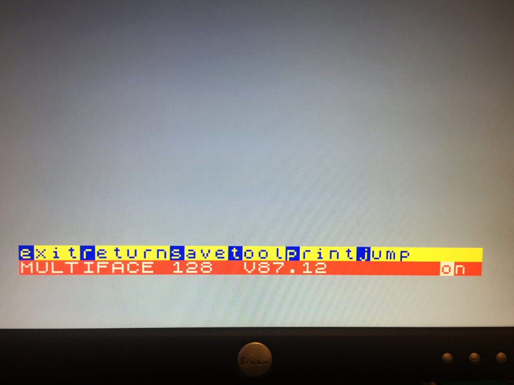
One press of the NMI button brings up the familiar menu. I have gone through the motions of testing the unit by initiating a tape save and poking 16384 with 255. It all seems OK. I have tested the interface with both a standard Microdrive and the fantastic vDrive ZX and both work correctly.
All the files for fabricating the Recreated Multiface 128 PCB v1 cabn be found here https://github.com/lostretrotapes/Romantic-Robot-Multiface-128-Re-Creation